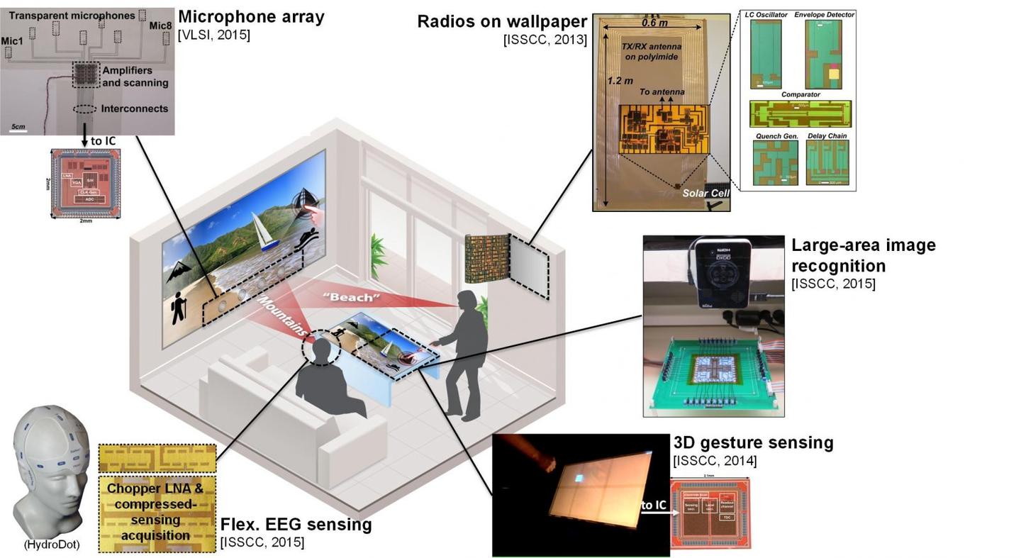
A primary insight driving our research is that a sensing technology has the ability to preserve specific structure in data to substantially enhance generalization of learning, and thereby advance cognitive capabilities. Following this insight, we pursue systems based on physically-integrated (PI) sensing. In contrast to remote sensing (e.g., vision) where the embedded signals coupled to each sensor (e.g., imager pixel) change in a dynamic environment with whatever is in the field of view, PI sensing directly associates sensors with physical objects, and, in doing so, enforces invariant semantic structure. For instance, in the area of human-interactive spaces, shown in the figure, semantic structure arises because the ways humans naturally interact with objects in their environments says something about the activities they are engaged in and the intentions they have. Today’s deep-learning models (e.g., convolutional neural networks) have achieved great success applied to remote sensing (e.g., vision), by first detecting what embedded signals are being sensed (i.e., by striding correlation filters within a layer) and then forming these into semantic features (i.e., by composition through layers). But, such ground-up learning contends with a large space of possibilities, requiring proportionately complex models, which are difficult to train and limit interpretability. Of course, we still make extensive use of remote sensing and deep learning. But we think about when and how to combine such approaches with PI sensing, to enable structure in sensing data towards regimes of faster learning, greater robustness, and increased adaptability/transferability.
So, PI sensing sounds good, but it raises two key technology challenges, which are big focus areas of our systems research:
- We must now deploy sensors, potentially on a very large scale, to capture the embedded signals arising from the many natural interactions between physical objects; but, such deployment must not be disruptive to those interactions and the information signals they generate. To address this, we research systems based on Large-Area Electronics (LAE), a technology capable of creating diverse, expansive, and form-fitting arrays of transducers.
- We must now perform continuous computations for learning, state estimation, and action planning from all of the sensor data; but, the embedded and distributed nature of that data raises critical resource-constraint challenges (energy, bandwidth, etc.). To address this, we research machine-learning algorithms together with new circuits and architectures, to exploit the statistical nature of both algorithms, for learning and inference, as well as energy-aggressive architectures, based on emerging devices and compute models.
Below are some examples from our experimental research in these areas; many of these examples combine results from our theoretical and algorithmic research.
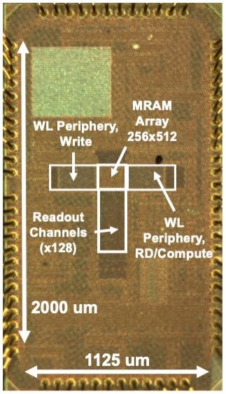
MRAM-based In-memory-computing Macro with Column-resistance boosting and ADC sharing: This paper presents a 128-kb in-memory computing (IMC) macro for fully row/column-parallel matrix-vector multiplication (MVM), implemented using a foundry MRAM in 22nm FD-SOI. Previous IMC in eNVM relied on RRAM with significantly higher resistance and resistance-state contrast than typical in foundry processes [1-3] or where parallelism was substantially reduced [4]. MRAM addresses distinct application requirements (e.g., temperature, radiation). This work advances previous MRAM IMC by improving area-normalized EDP by 60´ over [5] and by employing a standard high-density bit cell without additional devices, as in [6]. This is achieved via a readout architecture that performs column-resistance boosting, with integrated auto-zeroing, and conductance-to-current sampling, to simultaneously feed four IMC columns to a single ADC for conversion to 6-b outputs (highest ADC precision among eNVM IMC designs). [paper]
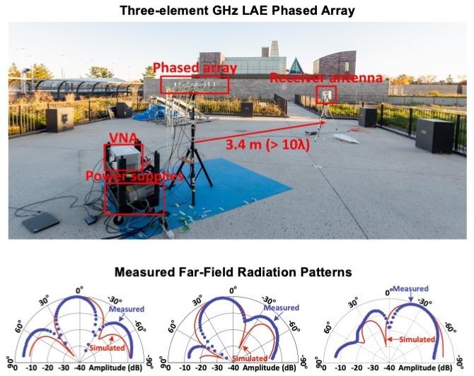
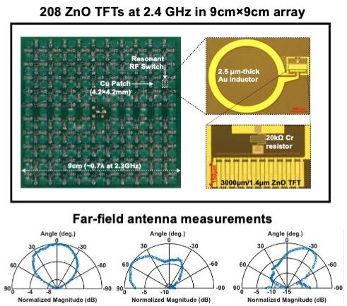
Large-area Giga-Hertz Phased-array Beamformer: Large-aperture electromagnetic phased arrays can provide directionally controlled radiation signals for use in applications such as communications, imaging and power delivery. However, their deployment is challenging due to the lack of an electronic technology capable of spanning large physical dimensions. Furthermore, applications in areas such as aviation, the Internet of Things and healthcare require conformal devices that can operate on shaped surfaces. Large-area electronics technology could be used to create low-cost, large-scale, flexible electromagnetic phased arrays, but it employs low-temperature processing that limits device- and system-level performance at high frequencies. Here we show that inductor–capacitor oscillators operating at gigahertz frequencies can be created from large-area electronics based on high-speed, self-aligned zinc-oxide thin-film transistors. The oscillator circuits incorporate frequency locking and phase tuning, which are required for electromagnetic phased arrays. We integrate our phase-tunable oscillators in a 0.3-m-wide aperture, creating a phased array system that operates at ~1 GHz and is capable of beamforming. [paper]
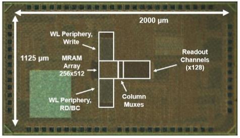
MRAM-based In-memory Computing Macro: This paper presents the first MRAM-based In-Memory-Computing (IMC) macro, implemented as a 128-kb array in an advanced-node 22nm FD-SOI technology. The design maximizes IMC row parallelism for energy efficiency and throughput, while addressing the critical challenges this raises, namely: high column currents; high output dynamic-range requirements; and large area of peripheral readout circuits. These are addressed through current-insensitive column multiplexing and high-sensitivity readout circuits, occupying 26% of the macro area. Residual IMC non-idealities, arising from statistical circuit variations, are modeled and incorporate in a chip-generalized one-time neural-network training algorithm, with CIFAR-10 image-classification accuracy demonstrated at 90.1%, equal to ideal digital computation. The design addresses the particularly high sensitivity required for MRAM-based IMC compared to other non-volatile memory technologies, while achieving area-normalized throughput of 758 GOPS/mm2 and energy efficiency of 5.1 TOPS/W for the macro. [paper]
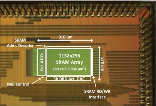
Fully-row/column Parallel In-memory-computing Macro with 5-b inputs: This work presents an in-memory computing (IMC) macro in 28nm for fully row/column-parallel matrix-vector multiplication (MVM), exploiting precise capacitor-based analog computation to extend from binary input-vector elements to 5-b input-vector elements, for 16x increase in energy efficiency and 5x increase in throughput. The 1152(row)x256(col.) macro employs multi-level input drivers based on a digital-switch DAC implementation, which preserve compute accuracy well beyond the 8-b resolution of the output ADCs, and whose area is halved via a dynamic-range doubling (DRD) technique. The macro achieves the highest reported IMC energy efficiency of 5796 TOPS/W and compute density of 12 TOPS/mm2 (both normalized to 1-b ops). CIFAR-10 image classification is demonstrated with accuracy of 91%, equal to the level of ideal SW implementation. [paper]
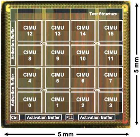
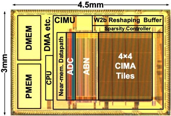
Scalable Programmable In-memory-computing Accelerator: This paper presents a scalable neural-network (NN) inference accelerator in 16nm, based on an array of programmable cores employing mixed-signal In-Memory Computing (IMC), digital Near-Memory Computing (NMC), and localized buffering/control. IMC achieves high energy efficiency and throughput for matrix-vector multiplications (MVMs), which dominate NNs; but, scalability poses numerous challenges, both technologically, going to advanced nodes to maintain gains over digital architectures, and architecturally, for full execution of diverse NNs. Recent demonstrations have explored integrating IMC in programmable processors, but have not achieved IMC efficiency and throughput for full executions. IMC substantially increases compute energy efficiency and HW density/parallelism, but retains the overheads of HW virtualization. The demonstrated architecture is co-designed with SW-mapping algorithms (encapsulated in a custom graph compiler), to provide efficiency across a broad range of mapping strategies, to overcome these overheads. [paper][paper]
Large-area 2.4 GHz Reconfigurable Antenna: Future IoT and 5G networks place significant new demands on antennas, where unguided EM waves are generated to access densely distributed sensor nodes. Reconfigurable antennas, capable of changing key parameters (directionality, frequency response, polarization), are starting to play a critical role, but are limited by the assembly of discrete RF components across the large antenna apertures typically desired. This work presents the design, and use in a reconfigurable antenna, of RF switches for 2.4 GHz-band wireless applications, based on large-area-electronics (LAE) zinc-oxide (ZnO) thin-film transistors (TFTs). ZnO TFTs can be fabricated monolithically on meter-scale and flexible substrates, as done in flat panel displays, but where their frequencies have been limited to 10’s of MHz. RF switch performance is enabled for ZnO TFTs (fabricated at flex-compatible temp. <200°C) via self-aligned processing, thick-composite gate electrodes, breakdown-safe biasing, and resonant operation, leveraging high-Q LAE inductors. [paper]
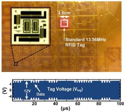
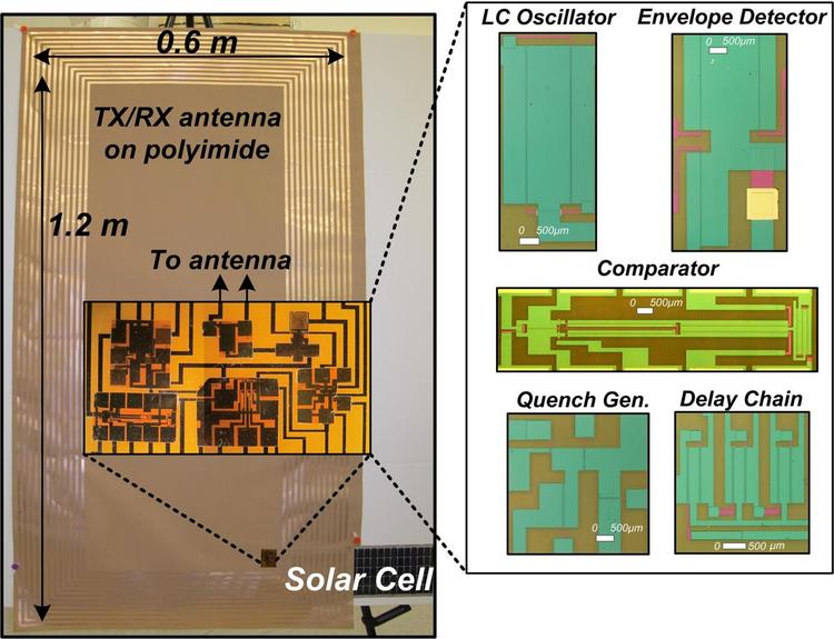
Large-area RFID Smart-tag Reader Sheet: This work presents a system that enables identification and localization of objects through an array of RFID-readers integrated into a thin sheet via large-area electronics, capable of lining everyday surfaces. We demonstrate a 5 x 5 active matrix of RFID readers based on thin-film transistor (TFT) LC oscillators, using in-house fabricated ZnO TFTs. The array is designed to read commercial ISO14443 13.56 MHz tags. The spatial resolution is set by the reader coil dimensions, which are 3.7 cm x 3.7 cm, for a maximum of 730 pixels/m2. Using a 2.4 cm x 2.4 cm tag the array achieves a vertical read range of 3 cm and lateral range of 1.6 cm at a readout speed of 5 ms per element (set by the commercial tag). Readout is accomplished by sensing the current via the shared VDD line of the array, reducing interfacing requirements as array size scales. The demodulated data has an amplitude of > 350 mV and the maximum power consumed by the reader array is < 280 mW. [paper]
Programmable Heterogeneous In-memory-computing Processor: Our previous work developed a high-SNR form of analog in-memory computing, based on precision capacitors. That lead to breakthrough scale and accuracy of in-memory-computing macros. This work exploits the high-SNR computation to form robust abstractions of in-memory-computing hardware, to enable architectural and software integration. A heterogeneous processor is presented, integrating bit-scalable (1-8 b) in-memory computing, with programmable near-memory digital SIMD computing, and an embedded CPU (RISC-V with DSP extensions). Additionally, the software stack is developed to design, train, and deploy neural-network models from PyTorch. The entire design is built into a PCB and development platform, for exploring wide-ranging applications of in-memory computing. [paper]
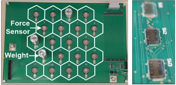
Large-area Tactile Sensing Skin based on In-sheet Compressed Sensing: Tactile sensing, and more generally embedded sensing, is characterized by close sensor coupling to embedded signals. This enables increased sensitivity and access to signal modalities not readily available through remote sensing. It also enables structure in the sensor data, thanks to signal-sensor invariance (in contrast, the specific signals acquired by remote sensors change dynamically). However, tactile sensing thus requires deploying many sensors, not because such sensors will all be activated at once, but rather to preserve such structure and close coupling. This work explores the creation of a large-scale tactile sensing skin, but where the attribute of sparse activation is exploited to ease sensor acquisition, by performing in-sensor computation of a compressed-sensing matrix projection over the sensor array. A hybrid CMOS-LAE system is presented for force sensing. [paper][paper]
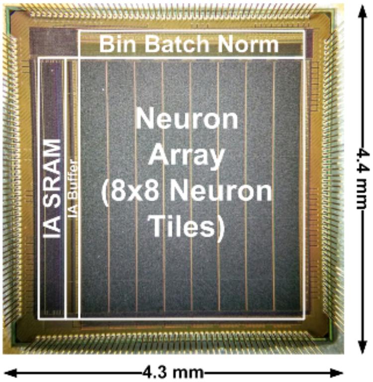
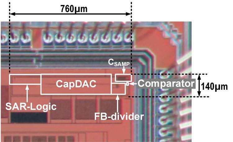
High-SNR Capacitor-based In-memory Computing: In-memory computing simultaneously addresses the energy/throughput of computation and data-accessing from memory, which can pose the critical bottleneck in data-intensive AI systems. It does this by accessing compute results over many bits stored in memory, rather than accessing individual bits one at a time. However, accessing compute results increases the required dynamic range, and thus restricts the SNR. The SNR is typically limited by nonidealities due to analog operation, employed in order to fit computation in the constrained bit cells. This work presents a high-SNR form of analog computation based on precision capacitors implemented using the standard metal stack in a CMOS technology. It thus achieves the highest accuracy and scale (2.8Mb macro) achieved for in-memory computing to date. [paper][paper]
Programmable Approximate Acceleration for Sensor-Inference: This work presents a heterogeneous microprocessor for low-energy sensor-inference applications. Hardware acceleration has shown to enable substantial energy-efficiency and throughput gains, but raises significant challenges where programmable computations are required, as in the case of feature extraction. To overcome this, a programmable feature- extraction accelerator (FEA) is presented that exploits genetic programming for automatic program synthesis. This leads to approximate, but highly structured, computations, enabling: 1) a high degree of specialization; 2) systematic mapping of programs to the accelerator; and 3) energy scalability via user-controllable approximation knobs. A microprocessor integrating a CPU with feature-extraction and classification accelerators is prototyped in 130-nm CMOS. [paper][paper]
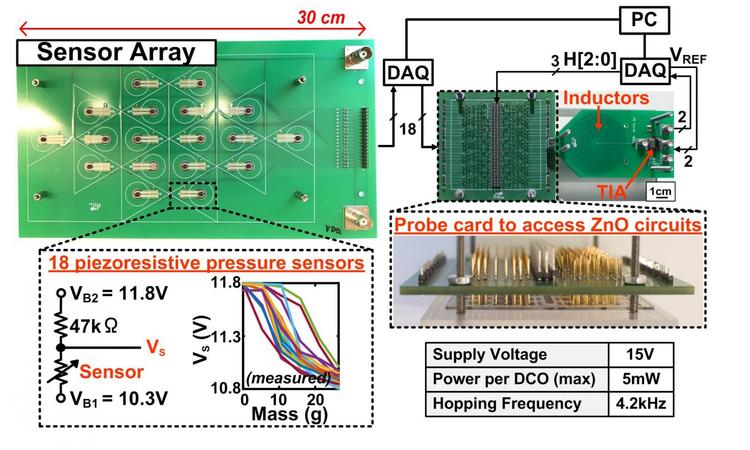
Frequency-Hopping DCO Architecture for Large-Area Pressure Sensing: Hybrid systems combine large-area electronics (LAE) with silicon-CMOS ICs for sensing and computation, respectively. In such systems, interfacing a large number of distributed LAE sensors with the CMOS domain poses a key limitation. This work presents an architecture that aims to greatly reduce both the number of physical connections and the time for accessing all of the sensors. Each sensor modulates the amplitude of a thin-film transistor (TFT) digitally controlled oscillator (DCO). All DCO outputs are combined, but each follows a unique frequency-hopping pattern (controlled by a code from CMOS), allowing recovery of the individual sensors. The architecture enables much greater scalability of sensors for a given number of connections than active-matrix and binary- addressing schemes. [paper][paper]
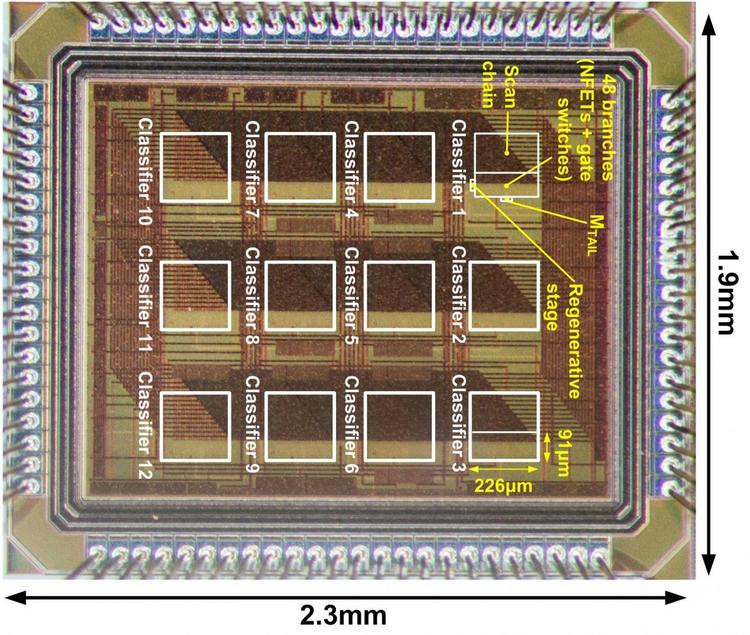
Direct Classification of Analog-sensor Data via Clocked Comparators:This work presents a system, where clocked comparators directly derive classification decisions from analog sensor signals, thereby replacing instrumentation amplifiers, ADCs, and digital MACs, as typically required. A machine-learning algorithm for training the classifier is presented, which enables circuit non-idealities as well as severe energy/area scaling in analog circuits to be overcome. Furthermore, a noise model of the system is presented and experimentally verified, providing a means to predict and optimize classification error probability in a given application. The noise model shows that superior noise efficiency is achieved by the comparator-based system compared with a system based on linear low-noise amplifiers. [paper]
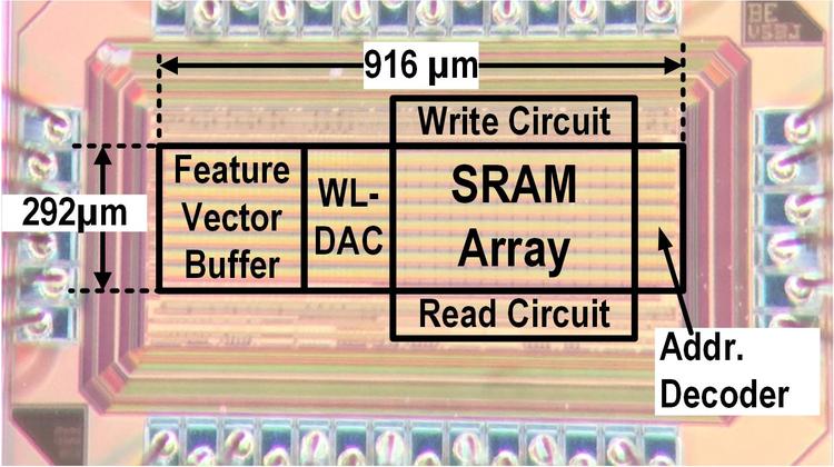
In-memory Computing Architecture for a Machine-learning Classifier:This work presents a machine-learning classifier, where computations are performed in a standard 6T SRAM array, which stores the machine-learning model. This eliminates the need for explicit memory accesses, instead performing accessing of a computational result over a large amount of data stored in the array, thus amortizing accessing energy/delay. Peripheral circuits implement mixed-signal weak classifiers via columns of the SRAM, and a training algorithm enables a strong classifier through boosting and also overcomes circuit non-idealities, by combining multiple columns. [paper][paper]
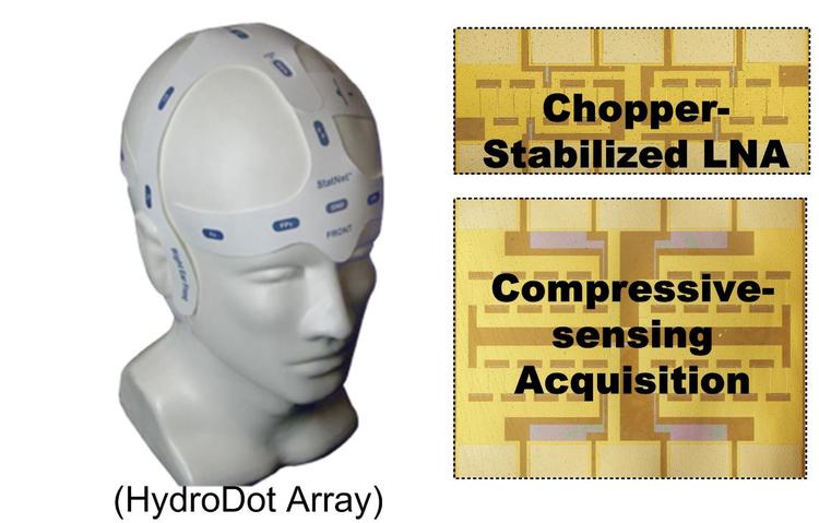
Flexible-electronics system for EEG acquisition and Processing: This work presents an electroencephalogram (EEG) acquisition and biomarker-extraction system based on flexible, thin-film electronics. There exist commercial, single-use, flexible, pre-gelled electrode arrays; however, these are fully passive, requiring cabling to transfer sensitive, low-amplitude signals to external electronics for readout and processing. This work presents an active EEG acquisition system on flex, based on amorphous silicon (a-Si) thin-film transistors (TFTs). The system incorporates embedded chopper- stabilized a-Si TFT low-noise amplifiers, to enhance signal integrity, and a-Si TFT compressive-sensing scanning circuits, to enable reduction of EEG data from many channels onto a single interface, for subsequent processing by a CMOS IC. [paper][paper]
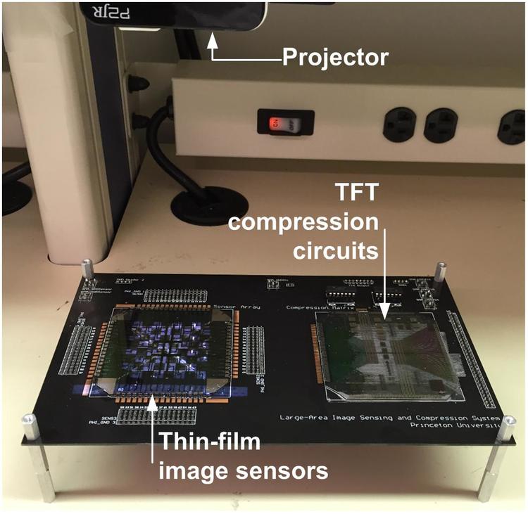
Large-area Image-sensing and Feature-extraction System: This work presents a sensing and compression system for image detection, based on large-area electronics (LAE). LAE allows us to create expansive, yet highly-dense arrays of sensors, enabling integration of millions of pixels. However, the thin-film transistors (TFTs) available in LAE have low performance and high variability, requiring the sensor data to be fed to CMOS ICs for processing. This results in a large number of interconnections, which raises system cost, and limits system scalability and robustness. To overcome this, the presented system employs random projection, a method from statistical signal processing, to compress the pixel data from a large array of image sensors in the LAE domain using TFTs. [paper]
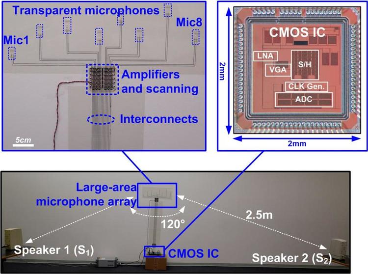
Large-area Microphone Phased Array: This work presents a system for reconstructing independent voice commands from two simultaneous speakers, based on an array of spatially distributed microphones. It adopts a hybrid architecture, combining large-area electronics (LAE), which enables a physically expansive array (>1 m width), and a CMOS IC, which provides superior transistors for readout and signal processing. The array enables us to: 1) select microphones closest to the speakers to receive the highest SNR signal; 2) use multiple spatially diverse microphones to enhance robustness to variations due to microphones and sound propagation in a practical room. Each channel consists of a thin-film transducer formed from polyvinylidene fluoride (PVDF), a piezopolymer, and a localized amplifier composed of amorphous silicon (a-Si) thin-film transistors (TFTs). Each channel is sequentially sampled by a TFT scanning circuit, to reduce the number of interfaces between the large-area electronics (LAE) and CMOS IC. [paper][paper][paper]
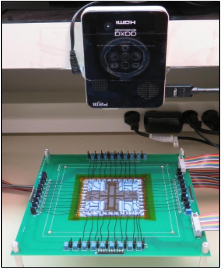
Large-area Image-sensing and Classification System: This work presents a large-area image-sensing and detection system that integrates, on glass, sensors and thin-film transistor (TFT) circuits for classifying images from sensor data. Large-area electronics (LAE) enables the formation of millions of sensors spanning physically large areas; however, to perform processing functions, thousands of sensor signals must be interfaced to CMOS ICs, posing a critical limitation to system scalability. This work presents an approach whereby image detection of shapes is performed using simple circuits in the LAE domain based on amorphous silicon (a-Si) TFTs. This reduces the interfaces to the CMOS domain. The limited computational capability of TFT circuits as well as high variability and high density of process defects affecting TFTs and sensors is overcome using a machine-learning algorithm known as error-adaptive classifier boosting (EACB) to form embedded weak classifiers. [paper][paper]
Matrix-multiplying ADC for Linear Feature Extraction and Classification in the A-D Process: In wearable and implantable medical-sensor applications, low-energy classification systems are of importance for deriving high-quality inferences locally within the device. Given that sensor instrumentation is typically followed by A-D conversion, this paper presents a system implementation wherein the majority of the computations required for classification are implemented within the ADC. To achieve this, first an algorithmic formulation is presented that combines linear feature extraction and classification into a single matrix transformation. Second, a matrix-multiplying ADC (MMADC) is presented that enables multiplication between an analog input sample and a digital multiplier, with negligible additional energy beyond that required for A-D conversion. [paper][paper][paper]
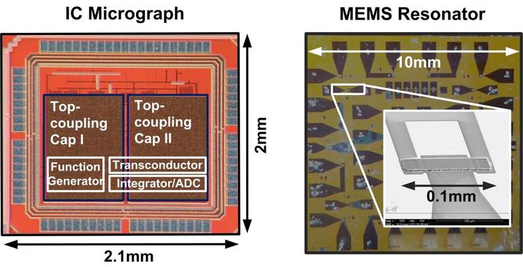
Frequency Readout of Post-processed Thin-Film MEMS Resonators:Thin-film MEMS resonators fabricated at low temperatures can be processed on CMOS ICs, forming high-sensitivity transducers within complete sensing systems. A key focus for the MEMS devices is increasing the resonant frequency, enabling, among other benefits, operation at atmospheric pressure. How- ever, at increased frequencies, parasitics associated with both the MEMS-CMOS interfaces and the MEMS device itself can severely degrade the detectability of the resonant peak. This work attempts to overcome these parasitics while providing isolation of the CMOS IC from potentially damaging sensing environments. To achieve this, an interfacing approach is proposed based on capacitive coupling across the CMOS IC passivation, and a detection approach is proposed based on synchronous readout. [paper][paper]
Large-Area 3D Multi-gesture Sensing System: This work presents a flexible 40×40cm2 gesture- sensing sheet for large-area interactive spaces. The system achieves out-of-plane sensing to 16cm. Self-capacitance readout of individual electrode pixels in a 4×4 array enables multiple gestures to be sensed simultaneously without ghost effects. For high-sensitivity readout, pixel self-capacitance is converted to frequency via high-Q LC oscillators formed from amorphous-silicon (a-Si) thin-film transistors (TFTs) and planar inductors patterned directly on flex. Frequency readout is then performed by a CMOS IC. Scalability in the number and scan rate of pixels is achieved by (1) inductively coupling all oscillators to the CMOS IC through a single interface, and (2) reading out all pixels in a row simultaneously in separated frequency channels. [paper]
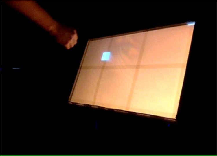
Large-Area 3D Gesture-sensing System: In this work, we present a 3D sensing system with 40×40cm2 area and sensing distance to 30cm. This distance is achieved via two approaches. First, capacitance sensing is performed via frequency modulation, and the sensitivity of frequency readout is enhanced by high-Q oscillators capable of filtering noise sources in the readout system as well as stray noise sources from display coupling. Second, the capacitance signal is enhanced by eliminating electrostatic coupling between the sensing electrodes and surrounding ground planes. [paper]
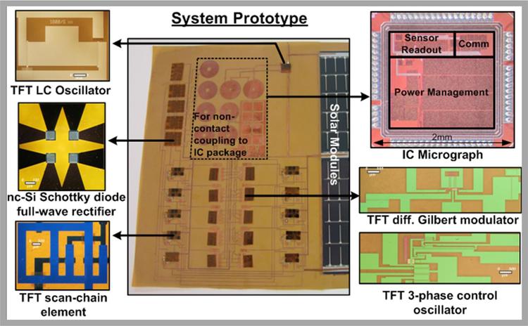
Self-powered Large-area Strain-Sensing Sheet for Structural Monitoring: This work presents a 2nd-generation system for high-resolution structural-health monitoring of bridges and buildings. The system combines large-area electronics (LAE) and CMOS ICs via scalable interfaces based on inductive and capacitive coupling. This enables architectures where the functional strengths of both technologies can be leveraged to enable large-scale strain sensing scalable to cm resolution yet over large-area sheets. The system consists of three subsystems: (1) a power-management subsystem, where LAE is leveraged for solar-power harvesting, and CMOS is leveraged for power conversion and regulation; (2) a sensing subsystem, where LAE is leveraged for dense strain sensing, and CMOS is leveraged for multi-sensor acquisition; and (3) a communication subsystem, where LAE is leveraged for long-range interconnects, and CMOS is leveraged for low-power transceivers. [paper][paper]
Large-area Strain-Sensing Sheet for Structural Monitoring: Early-stage damage detection for bridges requires continuously sensing strain over large portions of the structure, yet with centimeter-scale resolution. To achieve sensing on such a scale, this work presents a sensing sheet that combines CMOS ICs, for sensor control and readout, with large-area electronics (LAE), for many-channel distributed sensing and data aggregation. Bonded to a structure, the sheet thus enables strain sensing scalable to high spatial resolutions. In order to combine the two technologies in a correspondingly scalable manner, non-contact interfaces are used. Inductive and capacitive antennas are patterned on the LAE sheet and on the IC packages, so that system assembly is achieved via low-cost sheet lamination without metallurgical bonds. The LAE sheet integrates thin-film strain gauges, thin-film transistors, and long interconnects on a 50-μm-thick polyimide sheet, and the CMOS ICs integrate subsystems for sensor readout, control, and communication over the distributed sheet in a 130 nm process. [paper][paper]
Configurable Low-power Microprocessor for Medical-sensor Inference: Data-driven methods based on machine learning enable powerful frameworks for analyzing complex physiological signals in medical-sensor applications; however, these methods are not well supported by traditional DSPs. A general-purpose microprocessor is presented in 130nm CMOS that integrates configurable accelerators, enabling low-energy hardware to support the broadest range of machine-learning frameworks reported to date. In addition to computational energy, memory limitations due to the high-order data-driven models are overcome by an embedded compression/decompression accelerator, which reduces the memory footprint by 4× with overhead <8%. [paper]
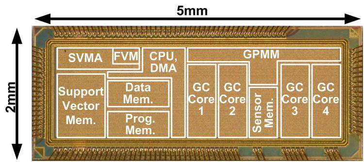
Low-power Microprocessor for Medical-sensor Inference: Low-power sensing technologies have emerged for acquiring physiologically indicative patient signals. However, to enable devices with high clinical value, a critical requirement is the ability to analyze the signals to extract specific medical information. Yet given the complexities of the underlying processes, signal analysis poses numerous challenges. Data-driven methods based on machine learning offer distinct solutions, but unfortunately the computations are not well supported by traditional DSP. This work presents a custom processor that integrates a CPU with configurable accelerators for discriminative machine-learning functions. A support-vector-machine accelerator realizes various classification algorithms as well as various kernel functions and kernel formulations, enabling range of points within an accuracy-versus-energy and -memory trade space. An accelerator for embedded active learning enables prospective adaptation of the signal models by utilizing sensed data for patient-specific customization, while minimizing the effort from human experts. [paper][paper]
Large-area Super-regenerative Radios on Wallpaper: This work presents a super-regenerative (SR) transceiver with integrated antenna on plastic that leverages the attribute of large area to create high- quality passives; this enables resonant TFT circuits at high frequencies (near ƒt) and allows for large antennas, maximizing the communication distance. The resulting carrier frequency is 900kHz, and the range is over 12m (at 2kb/s). This will enable sheets with integrated arrays of radio frontends for distributing a large number of communication links over large areas. [paper]
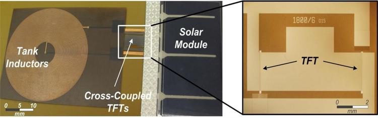
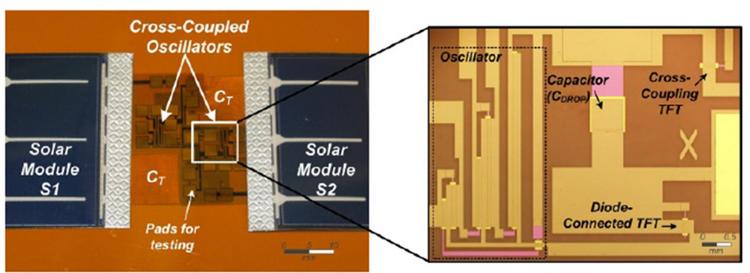
Large-area Wireless Charging System based on TFT LC Oscillators:This work presents an energy-harvesting system consisting of amorphous-silicon (a-Si) solar cells and thin-film-transistor (TFT) power circuits on plastic. Along with patterned planar inductors, the TFTs realize an LC- oscillator that provides power inversion of the DC solar- module output, enabling a low-cost sheet for inductively- coupled wireless charging of devices. Despite the low performance of the TFTs, the oscillator can operate above 2MHz by incorporating the device parasitics into the resonant tank. This enables increased quality factor for the planar inductors, improving the power-transfer efficiency and the power delivered. [paper]
Large-Area Wireless Charging System based on TFT Switching Power Inverters: With the explosion in the number of battery-powered portable devices, ubiquitous powering stations that exploit energy harvesting can provide an extremely compelling means of charging. This work presents a system on a flexible sheet that, for the first time, integrates the power electronics using the same thin-film amorphous-silicon (a-Si) technology as that used for established flexible photovoltaics. This demonstrates a key step towards future large-area flexible sheets which could cover everyday objects, to convert them into wireless charging stations. In this work, we combine the thin-film circuits with flexible solar cells to provide embedded power inversion, harvester control, and power amplification. This converts DC outputs from the solar modules to AC power for wireless device charging through patterned capacitive antennas. [paper]